
Level 2 Report
20 / 3 / 2025
Electronic Design
TASK 1 : MATLAB Onramp
In this task, we had to create a MATLAB (stands for Matrix Laboratory) account and obtain the MATLAB Onramp certification.
Learnings and Outcome:
- Learnt the different MATLAB commands
- How to import and visualize data
- The final project included analyzing the light recorded from a star to determine if it's moving towards or away from the earth.
Here is my certificate :

TASK 2 : 4 Bit ALU using CircuitVerse
CircuitVerse is a free, open-source platform which allows users to construct digital logic circuits online.
Learnings and Outcome-
Through this task, I learnt how to design a 4 bit Arithmetic and Logical Unit(ALU) which performs operations such as addition, subtraction and logical operations such as AND, OR and XOR. The multiplexer is used as the control unit in which according to the select lines, the operations are selected.
Here is the image of the circuit -

CircuitVerse link to view the working of the circuit.
TASK 3 : Convolution Countdown
Signal is a function of one or more independent variables, which contain some information.
Classification of Signals
- Continuous Time and Discrete Time Signals-
- A signal is said to be continuous when it is defined for all instants of time.
- A signal is said to be discrete when it is defined at only discrete instants of time.
- Deterministic and Non-deterministic Signals-
- Signals which can be defined exactly by a mathematical formula are known as deterministic signals.
- A signal is said to be non-deterministic if there is uncertainty with respect to its value at some instant of time. It cannot be described by a mathematical equation.
- Even and Odd Signals-
- A signal is said to be even when it satisfies the condition x(t) = x(-t).
- A signal is said to be odd when it satisfies the condition x(t) = -x(-t).
- Periodic and Aperiodic Signals-
- A signal is said to be periodic if it satisfies the condition x(t) = x(t + T) or x(n) = x(n + N).
- Energy and Power Signals-
- A signal is said to be energy signal when it has finite energy.
- A signal is said to be power signal when it has finite power.
System is a device or combination of devices, which can operate on signals and produces corresponding response. Input to a system is called as excitation and output from it is called as response.
Z transform -

Fourier Transform -

Outcome-
The task was to perform a simple Linear Convolution in MATLAB for two 4 sample discrete signals. I have calculated the convolution by using DFT and IDFT and verified the output by using the 'conv' function.
Here is the GitHub Link to view the code
Below is the Convolution in time domain -

This is the graph of the output -

TASK 4 : Cut, Pass, Repeat
A band pass filter is a device that permits frequencies within a specific range while attenuating those outside of it. The cascade connection of high pass and low pass filter makes another filter, known as the BPF.
- A second-order band-pass filter can be built using RLC components (resistor, inductor, capacitor) or using active components like operational amplifiers.
- The roll-off rate is -40 dB/decade (or -12 dB/octave) on either side of the passband.
- Centre frequency is given by
f = 1/ 2π√LC in passive RLC cicuits

Given Specifications-
OpAmp used - IC 747
Lower Cutoff frequency - 4kHz
Upper Cutoff frequency - 10kHz
Gain - 1.5 times (approx. 3.5dB)
Below is the design used for the circuit

Below is the circuit diagram -

Here is the simulated output waveform

TASK 5 : Buck and Boost Converters
A DC to DC converter is a power electronics circuit that efficiently converts a direct current from one voltage to another voltage. They offer several advantages over linear voltage regulators. Linear voltage regulators dissipate a lot of heat, and they have a very low efficiency compared with the switching regulators found in DC-DC converters.

- Switch is OFF --> Input voltage is 0
- Switch is ON --> Input voltage is 12V
Boost Converters
Boost converters increase the voltage of a power source. DC-DC boost converters is found in battery chargers or solar panels.
Here is a general schematic of a Boost converter -

- Switch is OPEN ---> a smaller current flows from the battery, through the inductor, through the diode and charging the capacitor.
- Switch is CLOSE ---> a larger current will flow from the battery, through the inductor and through the switch, the magnetic field of the inductor will expand, the potential across the inductor will be positive on the left and negative on the right.
- Switch is OPEN again ---> current through the circuit decreases, the magnetic field across the inductor will collapse, the polarity of the inductor changes.
Below is the circuit diagram in LT Spice -

Below is the output waveform -

It can be seen that the voltage across the load resistor(150ohms) boosts from 1.5V to 5V.
Buck Converter
Buck converters reduce the voltage of a power supply. Buck converters reduce the voltage by increasing the current.
Here is the general schematic of a Buck converter -

- Switch is CLOSED --> current increases, the magnetic field of the inductor will expand, the polarity of the inductor will be positive on the left and negative on the right, reduces the net voltage across the load.
- Switch is OPEN --> the magnetic field of the inductor will collapse, the current will flow from the inductor through the diode. This current will add to the current that flows during the OFF state. Thus, average current increases.
Below is the circuit diagram in LT Spice -

Below is the output waveform -

TASK 6 : SPICE Code
SPICE code is a text-based language used to describe electronic circuits and their components to a SPICE simulator. SPICE, which stands for "Simulation Program with Integrated Circuit Emphasis", is a software tool that engineers use to model and simulate the behavior of electronic circuits.
1. MOS Inverter
The SPICE code for an Inverter is -
Mnmos@0 out in gnd gnd NMOS L=0.6U W=3U
Mpmos@0 vdd in out vdd PMOS L=0.6U W=3U
vdd vdd 0 DC 5
vss gnd 0 DC 5
vin in 0 pulse(0 5 0 1n 1n 10n 20n)
.tran 0 200n
.include D:\Electric Binary\C5_models.txt
.END
Below is the circuit diagram in LT Spice -

Below is the simulated waveform of the output -

2. AND gate
The schematic circuit, SPICE code and the simulated output waveform for NAND is shown below-


The CMOS AND gate can be designed by extending the circuit of NAND gate with the use of an inverter.
The SPICE code for AND gate is -
VDD Vdd 0 DC 5
vss gnd 0 DC 5
VIN1 A 0 PULSE(0 5 0n 1n 1n 10n 20n)
VIN2 B 0 PULSE(0 5 0n 1n 1n 20n 40n)
M1 n1 A Vdd Vdd PMOS L=0.18u W=1u
M2 n1 B Vdd Vdd PMOS L=0.18u W=1u
M3 n1 A n2 0 NMOS L=0.18u W=0.5u
M4 n2 B 0 0 NMOS L=0.18u W=0.5u
M5 Y n1 Vdd Vdd PMOS L=0.18u W=1u
M6 Y n1 0 0 NMOS L=0.18u W=0.5u
.TRAN 0.1n 100n
.include D:\Electric Binary\C5_models.txt
.END
Below is the circuit diagram for AND gate in LT Spice -

Below is the simulated output waveform -

3. OR Gate
The schematic circuit, SPICE code and the simulated output waveform for NOR is shown below-


The CMOS OR gate can be designed by extending the circuit of NOR gate with the use of an inverter.
The SPICE code for OR gate is -
VDD Vdd 0 DC 5
VSS gnd 0 DC 5
VIN1 A 0 PULSE(0 5 0n 1n 1n 10n 20n)
VIN2 B 0 PULSE(0 5 0n 1n 1n 20n 40n
M1 n1 A Vdd Vdd PMOS L=0.18u W=1u
M2 n1 B Vdd Vdd PMOS L=0.18u W=1u
M3 n1 A 0 0 NMOS L=0.18u W=0.5u
M4 n1 B 0 0 NMOS L=0.18u W=0.5u
M5 Y n1 Vdd Vdd PMOS L=0.18u W=1u
M6 Y n1 0 0 NMOS L=0.18u W=0.5u
.TRAN 0.1n 100n
.include D:\Electric Binary\C5_models.txt
.END
Below is the circuit diagram for OR gate in LT Spice -

Below is the simulated output waveform -

TASK 7 : Voltage Multiplier
A voltage multiplier is an electronic circuit that uses diodes and capacitors to convert a lower AC voltage to a higher DC voltage. It generates an output voltage that is a multiple of the input voltage.
There are 4 types of voltage multiplier circuits -
- Half Wave Voltage Doubler
- Full Wave Voltage Doubler
- Voltage Tripler
- Voltage Quadrupler
Advantages -
- Helpful for compact designs
- Low cost
- Simple construction
- High voltage output
Disadvantages -
- Limited to low power applications
- Gives voltage ripple
- Limited frequency range
- Sensitive to load variations
Applications -
- Cathode Ray Tubes displays
- Photo multiplier tubes
- X Ray generators
Below is the circuit diagram for a voltage multiplier/doubler -

Below is the waveform of the voltage across C4 -

As it can be seen, the voltage doubles from 9v to 18V (approx)
Working-
- The 555 timer IC, in combination with the 5nF capacitor and 33K resistor, produces a square wave at its output i.e. at Pin-3.
- When the output of 555 timer IC is at 0V (negative voltage), the 22uF capacitor charges through the diode.
- When the output of 555 timer IC is at positive voltage, the voltage across the 22uF capacitor will be in series with the voltage from the output of 555 timer IC.
- Since two voltage sources in series will add up, the voltage at the other end of 22uF capacitor will be equal to voltage at the output of 555 timer IC + the voltage across the capacitor.
- So by now we have a voltage that is approximately double the input voltage. At the end a 22uF capacitor is connected to smoothen out the output.
- The above capacitors and diodes arrangements is named as a capacitor charge pump.
Below is the image of Voltage Tripler -
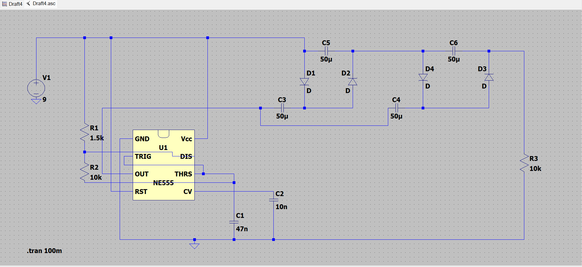
Below is the output waveform -
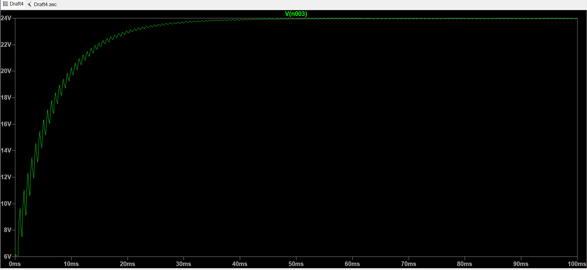
The voltage further triples from 9 V to 27 V (approx).
TASK 8 : PCB Revolution -
The objective of this task was to learn the basics of PCB (Printed Circuit Board) Designing. We had to apply for the Altium student license and complete the Altium Student Lab PCB coursework.
The coursework included the following -
- Introduction to PCB Design - Basic terms like schematic sheets, bill of materials, PCB layout and more, were introduced.
- Schematics and Libraries - This section included the anatomy of a schematic, the types of schematics, how to select and place components, and transitioning to a layout.
- PCB Layout - This consisted of PCB Design and manufacturing process, PCB design workflow, Stackup design, the design rules to be followed, and the Layout process.
- Routing and Basic Signal Integrity - It included Designing and Routing with Vias, routing different types of signals, routing rules for impedance control, and the concept of EMI.
- PCB Manufacturing - It explains about the preparation required for manufacturing, the topic of panelization, PCB Fabrication process, PCB assembly process.
- Fundamentals of Purchasing and Supply Chain - This unit explained the fundamentals of purchasing.
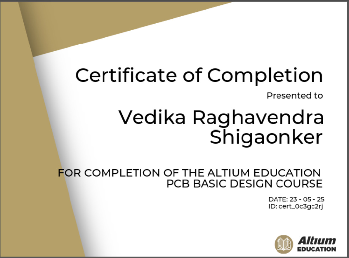
Here is my certificate of completion -
Click here for part 2 of the report