
Nawaz's D&P Level 1 Report
12 / 10 / 2026
This report highlights three selected tasks completed as part of MARVEL D&P Level 1: a 555 Timer voltage multiplier, a 4-bit Arithmetic Logic Unit (ALU), and PCB design using KiCad. The circuit designs, calculations, simulation results, and screenshots are included below. The titles of the remaining completed tasks and a link to the complete GitHub report are provided at the end.
Task 04 - From Low to Woah!
Objective
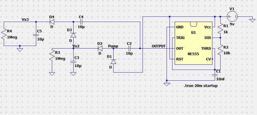
To understand the working of voltage multipliers using capacitor charge pumps driven by a 555 Timer IC and generate higher DC voltages from a 9V input supply.
Task
- Design a voltage multiplier circuit to increase a 9V DC input.
- Use capacitor charge-pump stages driven by a 555 Timer IC.
- Observe the voltage multiplication effect through simulation.
- Verify the output voltages obtained at each stage.
Platform Used: LTSpice
Theory
A voltage multiplier is a circuit that converts a low DC voltage into a higher DC voltage using capacitors and diodes. Instead of using a transformer, the circuit stores and transfers charge between capacitors during each switching cycle.
The 555 Timer IC is configured in astable mode to generate a continuous square-wave signal. This signal repeatedly charges and discharges the capacitors through the diode network.
As the capacitors charge, their voltages add together, resulting in a higher output voltage. By cascading multiple charge-pump stages, the output voltage can be increased further.
Components Used
- NE555 Timer IC
- Diodes
- Capacitors
- Resistors
- 9V DC Supply
Procedure
- Configured the 555 Timer IC in astable mode to generate a square-wave signal.
- Connected a capacitor-diode network to form the first voltage multiplier stage.
- Simulated the circuit and observed the voltage increase at the intermediate node.
- Added another multiplier stage by cascading additional capacitors and diodes.
- Simulated the complete circuit in LTSpice.
- Measured the voltages at different stages and analysed the output waveform.
Observations
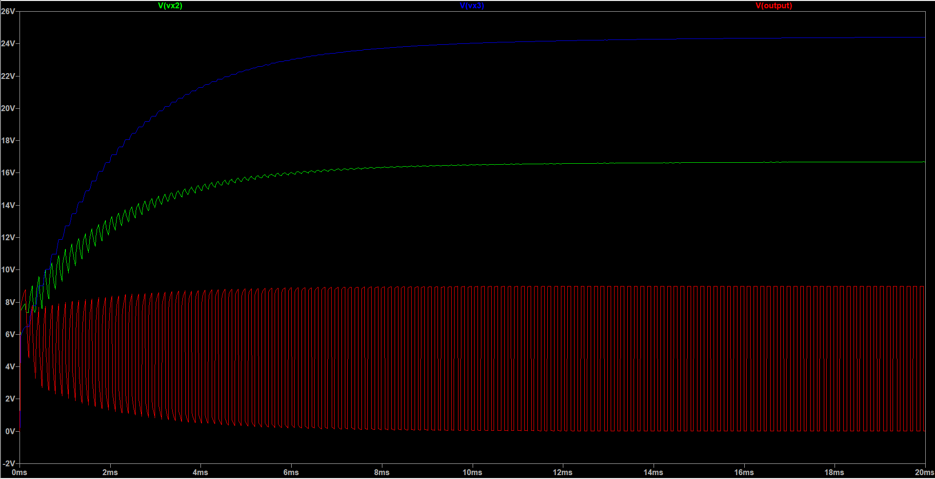
- The first voltage multiplier stage increased the input voltage from 9V to approximately 16.6V.
- The second multiplier stage further increased the voltage to approximately 24.4V.
- The output voltage gradually increased as the capacitors charged.
- Small ripple voltages were observed due to the charging and discharging cycles of the capacitors.
Results
- Successfully implemented a voltage multiplier circuit using a 555 Timer IC.
- Obtained approximately 16.6V at the first multiplier stage from a 9V input supply.
- Obtained approximately 24.4V at the final multiplier stage by cascading charge-pump stages.
- Verified the voltage multiplication effect through LTSpice simulation.
Learning Outcomes
- Understood the working principle of capacitor charge pumps.
- Learned how diodes control the direction of current flow during charging cycles.
- Understood how cascading stages increases the output voltage.
- Gained experience in simulating voltage multiplier circuits using LTSpice.
- Learned the practical effects of diode voltage drops and output ripple.
555 Timer Voltage Multiplier Circuit
Simulation Results
Task 06 - 4 Bits to Rule Them All
Objective
To design and implement a 4-bit Arithmetic Logic Unit (ALU) capable of performing arithmetic and logical operations using basic digital logic components in CircuitVerse.
Tools Used
- CircuitVerse
- Digital Logic Design Concepts
Task
Design and implement a 4-bit ALU capable of performing:
- 4-bit Addition
- 4-bit Subtraction using 2's Complement
- 4-bit AND Operation
- 4-bit OR Operation
- 4-bit XOR Operation
- 4-bit NOT Operation (Bonus)
The ALU should use control signals to select the required operation and display the corresponding output.
Theory
An Arithmetic Logic Unit (ALU) is the computational core of a digital system. It performs arithmetic and logical operations on binary data.
A 4-bit ALU accepts two 4-bit inputs and processes them based on control signals. Arithmetic operations such as addition and subtraction are performed using adder circuits, while logical operations are implemented using logic gates.
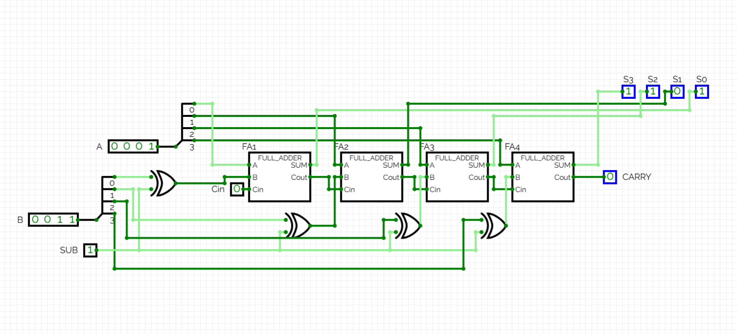
Subtraction is achieved using the 2's complement method, where the second operand is inverted and a carry of 1 is added. This allows subtraction to be performed using the same adder hardware used for addition.
Control lines are used to select the desired operation, making the ALU a programmable combinational circuit.
Procedure
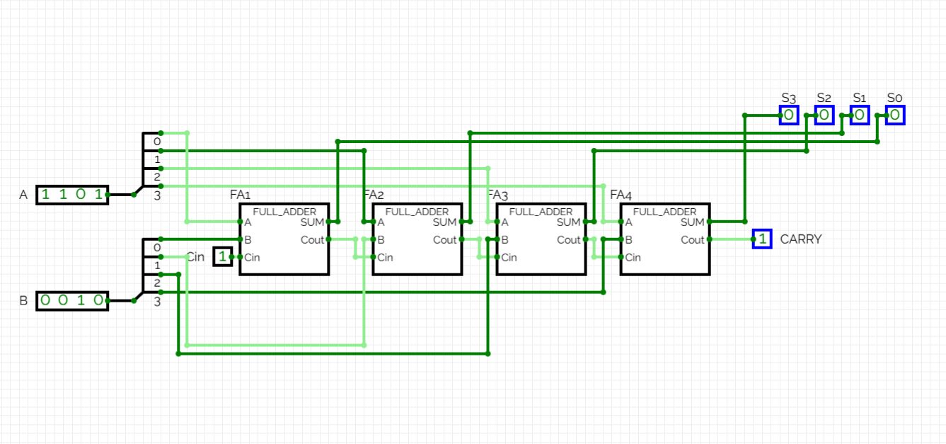
- Designed a 4-bit ripple carry adder using Full Adders.
- Verified correct carry propagation and arithmetic addition.
- Modified the adder circuit to perform subtraction using the 2's complement technique.
- Implemented 4-bit AND, OR, XOR and NOT circuits using logic gates.
- Designed multiplexing logic to select the required operation based on control signals.
- Combined all arithmetic and logical blocks into a single ALU architecture.
- Tested all possible operations with different input combinations.
- Verified outputs for correctness.
Individual Functional Blocks
4-Bit Adder
4-Bit Adder/Subtractor
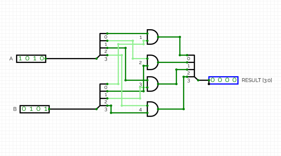
4-Bit AND
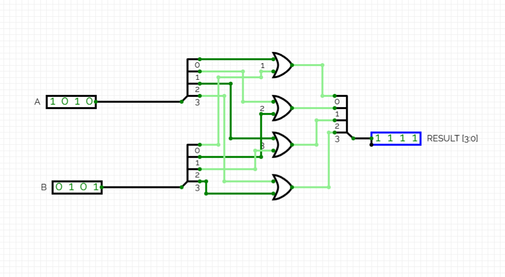
4-Bit OR
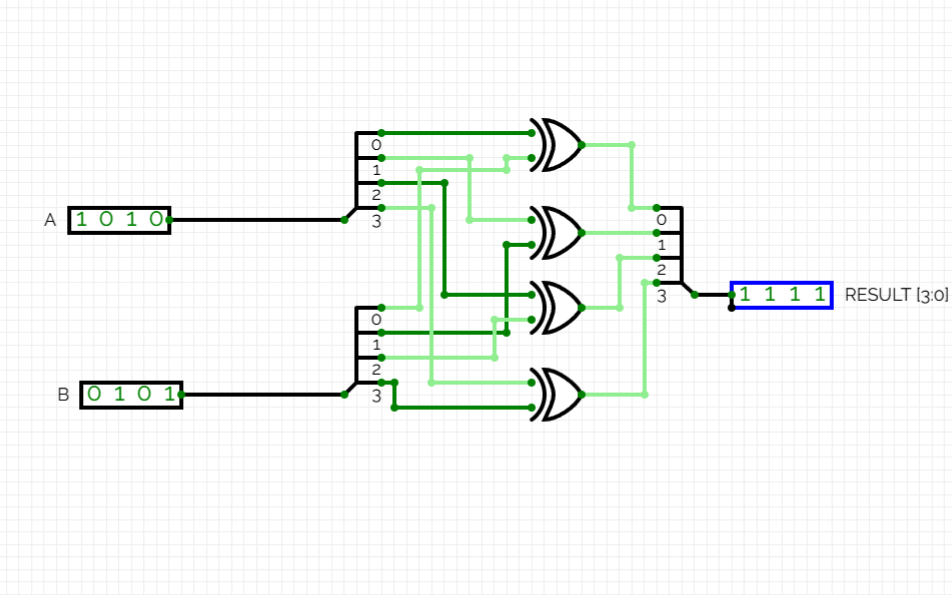
4-Bit XOR
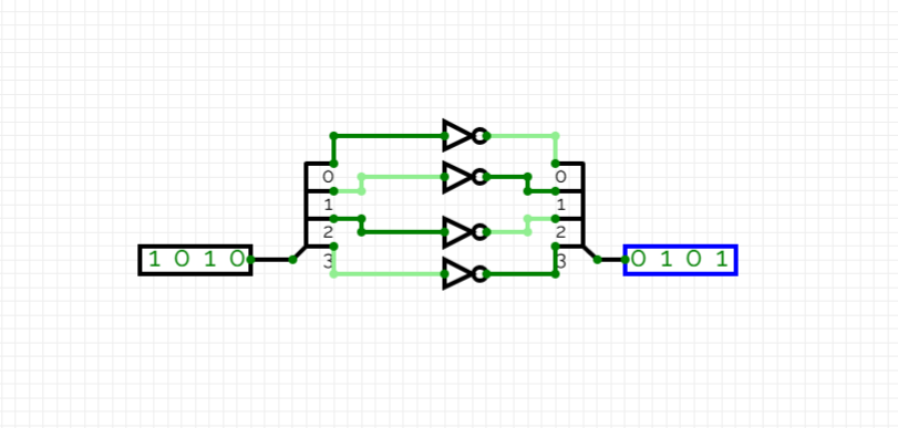
4-Bit NOT
ALU Design (Using 2 Select Lines)
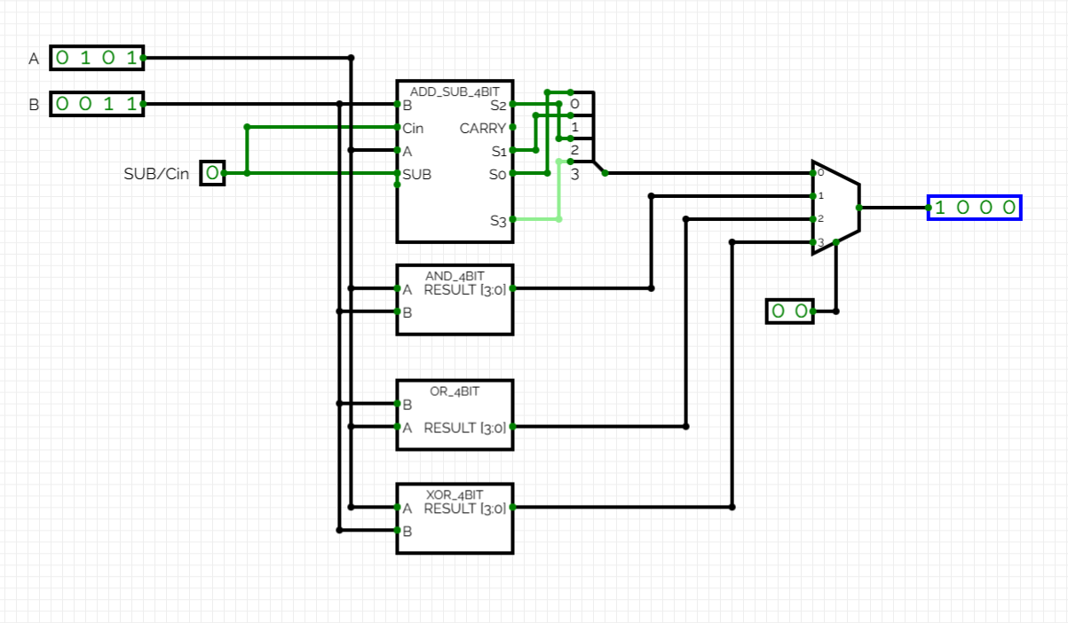
Final 4-Bit ALU
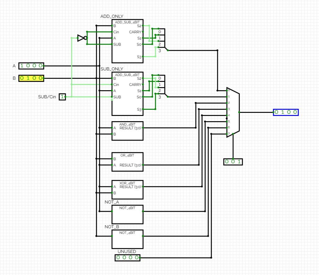
Sample Verification Table
For testing the ALU, the following inputs were used:
| Input A | Input B |
|---|---|
| 1011 | 0110 |
| Select Lines | Operation | Output |
|---|---|---|
| 000 | Addition (A + B) | 0001 (Carry = 1) |
| 001 | Subtraction (A - B) | 0101 |
| 010 | AND | 0010 |
| 011 | OR | 1111 |
| 100 | XOR | 1101 |
| 101 | NOT A | 0100 |
The obtained outputs matched the expected results for all tested operations.
Working
- The 4-bit adder performs binary addition of two 4-bit inputs.
- The subtractor uses XOR gates and a carry-in of 1 to generate the 2's complement of the second operand.
- AND, OR and XOR blocks perform bitwise logical operations.
- The NOT block inverts each bit of the selected input.
- Control lines determine which operation output is routed to the final ALU output.
- The ALU produces the required result while also handling carry generation during arithmetic operations.
Results
- Successfully designed a 4-bit Adder.
- Successfully implemented a 4-bit Adder/Subtractor using 2's complement.
- Successfully implemented 4-bit AND, OR and XOR logic operations.
- Successfully implemented 4-bit NOT operation.
- Successfully integrated all functional blocks into a single ALU architecture.
- Verified correct operation through simulation and testing in CircuitVerse.
- Verified ALU functionality using test inputs A = 1011 and B = 0110 for all supported operations.
Learning Outcomes
- Understood the architecture of an ALU.
- Learned how arithmetic operations are implemented using Full Adders.
- Understood subtraction using the 2's complement method.
- Learned implementation of bitwise logical operations.
- Gained experience in hierarchical digital circuit design.
- Learned how control signals are used to select ALU operations.
- Improved understanding of combinational logic system design.
CircuitVerse Project
CircuitVerse Project Link:
Conclusion
The 4-bit ALU was designed and tested in CircuitVerse. The circuit combines arithmetic and logical functional blocks and uses control signals to select the required operation. Testing with sample inputs helped verify the output of each implemented operation.
Task 09 - The PCB Revolution
Objective
To learn the basics of PCB designing and understand the process of converting a circuit schematic into a routed PCB layout.
Tools Used
- KiCad 10.0.1
Procedure
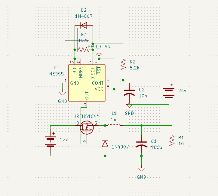
- Created the circuit schematic and assigned footprints to the components.
- Transferred the design to the PCB Editor and arranged the components.
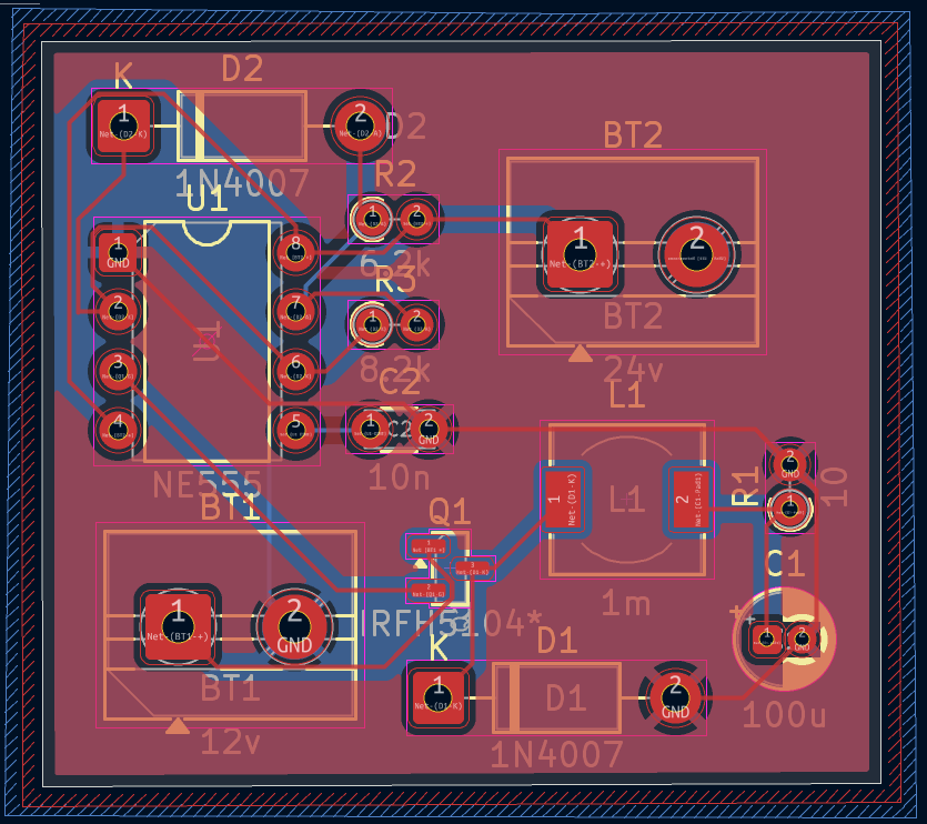
- Created the PCB layout and routed the connections.
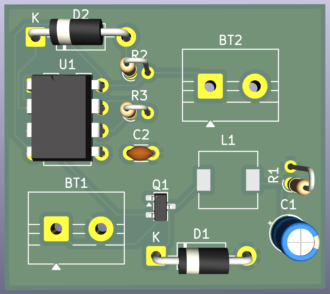
- Checked the unrouted and routed layouts and viewed the final PCB in 3D.
PCB Schematic (Buck Converter)
PCB Layout
Unrouted PCB
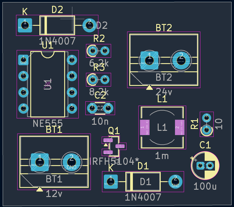
Routed PCB
3D PCB View
Learning Outcomes
- Understood the workflow from schematic design to PCB layout.
- Learned component placement and track routing.
- Understood the difference between unrouted and routed PCBs.
- Explored the 3D view of the PCB in KiCad.
Conclusion
This task helped me understand the basic PCB design workflow in KiCad, from creating the schematic to routing the PCB and inspecting its 3D representation.
Remaining Completed Tasks
The following tasks are also documented in the full report:
- Task 01 - Engineer's Swiss Army Knife — MATLAB Onramp
- Task 02 - SPICEy Code — MOS Inverter, AND Gate and OR Gate using LTSpice
- Task 03 - Cut, Pass, Repeat — Band Pass Filter
- Task 05 - The Power Shuffle: Buck-Boost Edition — Buck and Boost Converters
- Task 07 - Your Logic, Preloaded — 4×1 XOR Lookup Table
- Task 08 - Whose Array Is It Anyway? — PAL, PLA and Smart-Home Controller
For the detailed explanations, calculations, circuit diagrams, screenshots, and results of these tasks, please refer to the complete GitHub report:
GitHub Report:
https://github.com/nawazhussainhs/Marvel_Level_1_Report