
24 / 3 / 2025
Task 1: Cut, Pass and Repeat
Objective: To learn about Band Pass Filters and to design a second order band pass filter using IC747 that amplifies the signal to roughly 1.5 times the original signal of the Cutoff range between 4kHz and 10kHz.
Platform: LTSpice
What is a Bandpass filter?
A bandpass filter is an electronic circuit that allows signals within a specific frequency range to pass through while attenuating frequencies outside this range. A second order filter is used to provide better roll-off rate and is designed by using Opamps, resistors and capacitors. Here, the design is based on Sallen Key topology, which is the most commonly used architecture for second order filters.
Specifications and values
| Specification | Value | ||
|---|---|---|---|
| Passband gain | roughly 1.5 (≈3.5 dB) | ||
| Lower cutoff frequency | 4KHz | ||
| Upper cutoff frequency | 10KHz | ||
| OpAmp | IC747 |
Circuit Diagram

Design Specifications

Output

Passband gain is approximately equal to 1.5 or 3.5dB
Task 2: SPICEy Code
- Objective: To learn SPICE code and write basic SPICE code for a MOS inverter, AND and OR Gates
- Platform: LTSpice
What is Spice Code?
SPICE code refers to a circuit description written in the LTSPICE (Simulation Program with Integrated Circuit Emphasis) language. It is a tool used for simulating analog circuits. It is a textual description of an electrical circuit containing,
- Components: resistors, capacitors, transistors, etc.
- Nodes: connection points
- Models: behavior definitions for components like semiconductors
- Simulation commands: types of analysis like DC, AC, transient
Example
- The first column is the element. (R1)
- The next two columns indicate between which nodes the element is present. (R1 is present between node 2 and 1)
- The next column indicates the value. (R1 is between node 2 and 1 of the value 2k ohm)
- Node 0 indicates that the one end of the element is connected to the ground.
MOS INVERTER
M1 output input 0 0 CMOSN l=180n w=200n
M2 Vdd input output Vdd CMOSP l=180n w=400n
- this section defines the two mosfet's specifications.
- Format: (Transistor name) (Drain) (Gate) (Source) (Bulk) (Model) (Channel length) (Channel width)
Vin input 0 PULSE(0 1.8 2.5n 500p 500p 10n 20n)
- this section indicates the input waveform
V1 Vdd 0 1.8
- it is the power supply for the inverter
.model NMOS NMOS
.model PMOS PMOS
.lib C:\Users\venus\OneDrive\Documents\LTspiceXVII\lib\cmp\standard.mos
.include tsmc018.lib
- these sections are used for the declarations of the characteristics of the components used in the circuit.
- .include tsmc018 text file includes the specifications of most of the components, especially CMOSN and CMOSP
.tran 40n
- runs the transient analysis - behaviour of output with respect to input
.backanno
.end
- marks the end of the spice code

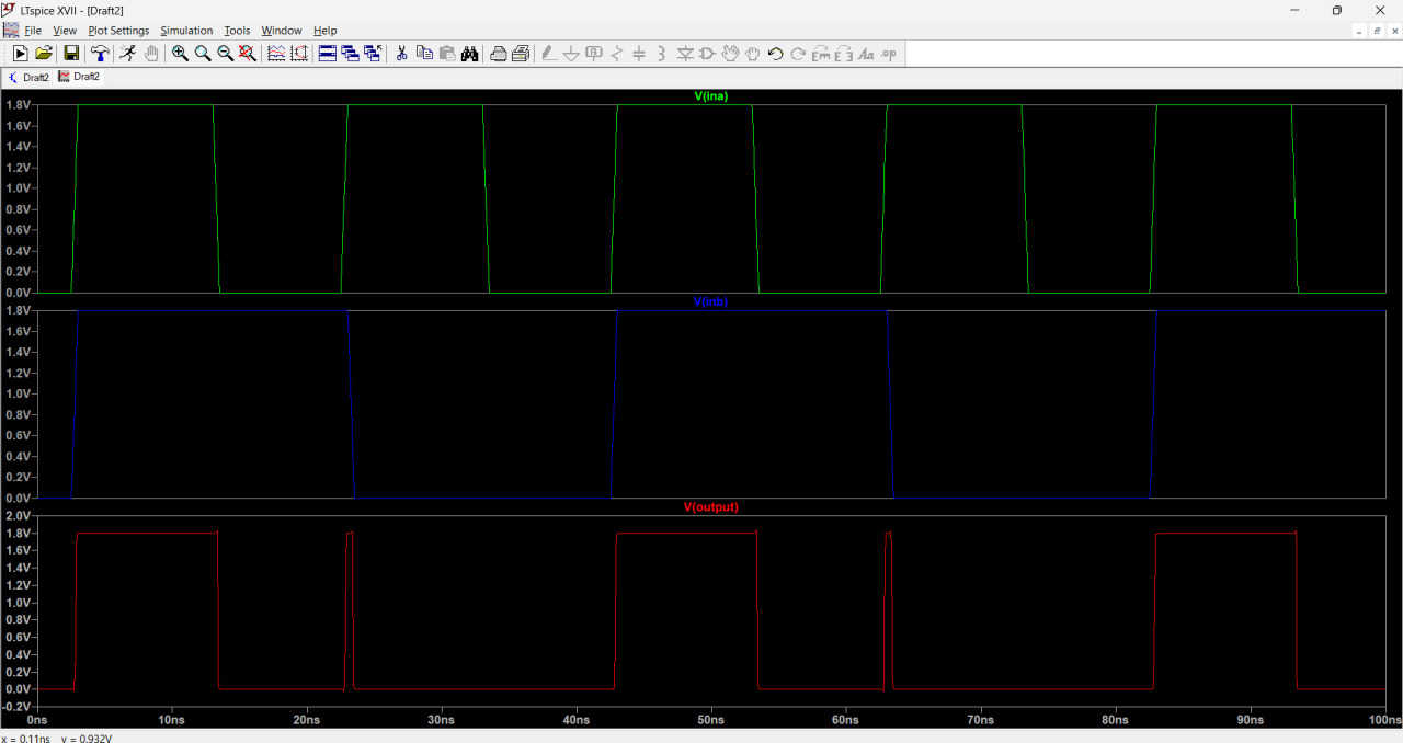
MOS AND
M1 VDD inA NAND_out VDD CMOSP l=180n w=400n
M2 VDD inB NAND_out VDD CMOSP l=180n w=400n
M3 NAND_out inA P001 N001 CMOSN l=180n w=200n
M4 P001 inB 0 N001 CMOSN l=180n w=200n
M5 VDD NAND_out output VDD CMOSP l=180n w=400n
M6 VDD NAND_out output VDD CMOSP l=180n w=400n
M7 output NAND_out P002 N002 CMOSN l=180n w=200n
M8 P002 NAND_out 0 N002 CMOSN l=180n w=200n
- Specifications of the transistors used
VDD VDD 0 1.8
- power source
VA inA 0 PULSE(0 1.8 2.5n 500p 500p 10n 20n)
VB inB 0 PULSE(0 1.8 2.5n 500p 500p 20n 40n)
- inputs A and B
.model NMOS NMOS
.model PMOS PMOS
.lib C:\Users\venus\OneDrive\Documents\LTspiceXVII\lib\cmp\standard.mos
.include tsmc018.lib
- component characteristics declaration
.tran 100n
- transient analysis
.backanno .end
- marks the end of code
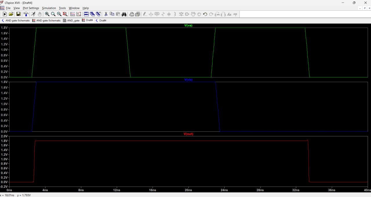
MOS OR
M1 VDD VA P001 VDD CMOSP l=180n w=400n
M2 P001 VB NOR_out VDD CMOSP l=180n w=400n
M3 NOR_out VA 0 0 CMOSN l=180n w=200n
M4 NOR_out VB 0 0 CMOSN l=180n w=200
M5 VDD NOR_out P002 VDD CMOSP l=180n w=400n
M6 P002 NOR_out Out VDD CMOSP l=180n w=400n
M7 Out NOR_out 0 0 CMOSN l=180n w=200n
M8 Out NOR_out 0 0 CMOSN l=180n w=200n
- Specifications of the transistors used
VDD VDD 0 1.8
- power source
V2 VA 0 PULSE(0 1.8 2.5n 500p 500p 10n 20n)
V3 VB 0 PULSE(0 1.8 2.5n 500p 500p 20n 40n)
- inputs A and B
.model NMOS NMOS
.model PMOS PMOS
.lib C:\Users\venus\OneDrive\Documents\LTspiceXVII\lib\cmp\standard.mos
.include tsmc018.lib
- component characteristics declaration
.tran 40n
- transient analysis
.backanno
.end
- marks the end of code
Task 3: From Low to Woah!
- Objective: Voltage multiplier using capacitor pumps and a 555 Timer IC and pump up 9V to 18V at first, then cascade the pump to get 27V.
- Platform: LTSpice
What is a Voltage Multiplier?
A voltage multiplier is a circuit that increases the voltage level without using a transformer. It uses diodes and capacitors arranged in a specific configuration to generate multiples of the input voltage like 2x, 3x etc. These circuits rely on Clock like signals or AC signals to pump charge through the diodes and store energy in capacitors.
Voltage Doubler
A voltage doubler is a circuit that converts an AC input voltage to a DC voltage approximately twice the peak input voltage.
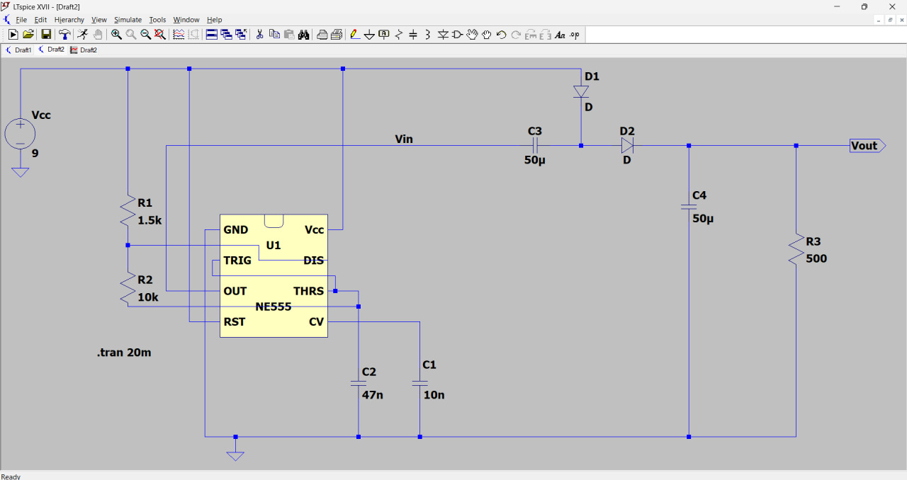
1. 555 Timer as an Astable Multivibrator
- Components: R1 = 1.5kΩ, R2 = 10kΩ, C2 = 47nF, C1 = 10nF
- The 555 timer generates a square wave at the output.
- This output square wave (Vin) is used to drive the voltage doubler section.
2. Voltage Doubler Stage (Charge Pump)
- Components: D1, D2, C3 = 50µF, C4 = 50µF
Operation:
- During LOW phase of the square wave: Capacitor C3 charges through D1 from the 555 output.
- During HIGH phase of the square wave: The charged C3 gets added to the supply voltage (Vcc = 9V) via D2, transferring energy to C4.
- Output voltage Vout ≈ 2 × Vcc = ~18V
- Output voltage is not exactly 18 V due to voltage drops of Diodes (~0.7 V)

Voltage Tripler
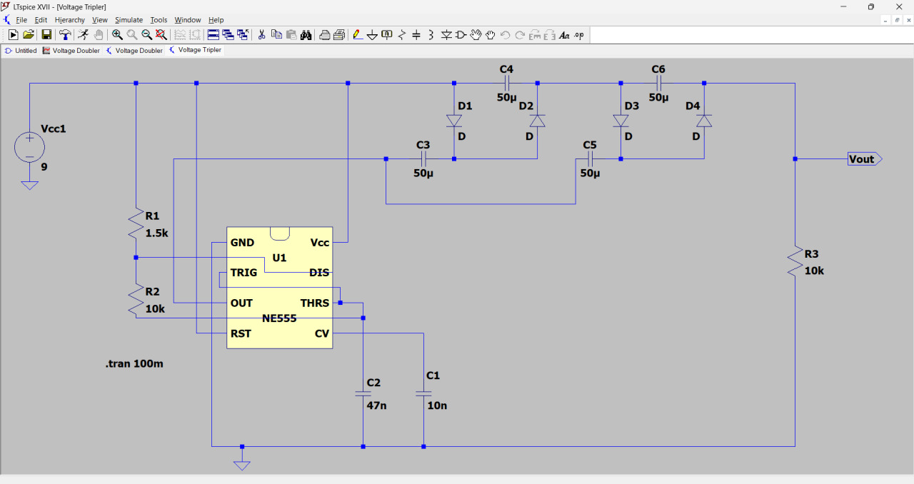
555 Timer as Oscillator
- Components: R1 = 1.5kΩ, R2 = 10kΩ, C2 = 47nF, C1 = 10nF
- The 555 timer generates a square wave at the output.
- This output square wave (Vin) is used to drive the voltage tripler section.
**Voltage Tripler Section
Stage 1: Voltage Doubling
- When the square wave from the 555 timer output goes high, capacitor C3 charges through diode D1 up to the supply voltage (~9V).
- When the output goes low, the bottom of C3 is pulled to ground, and since C3 holds a charge of 9V, its **top terminal now rises to 18V.
- This 18V is passed through diode D2 and stored in capacitor C4, giving the doubled stage (~18V).
Stage 2: Tripling
- Now, in the next positive cycle of the square wave, capacitor C5 charges through diode D3 up to the same 9V.
- On the negative edge, the bottom of C5 goes low, and its top is again raised by 9V, resulting in ~27V at its top.
- This 27V is passed through diode D4 and stored in capacitor C6, which now holds the tripled voltage (~27V).
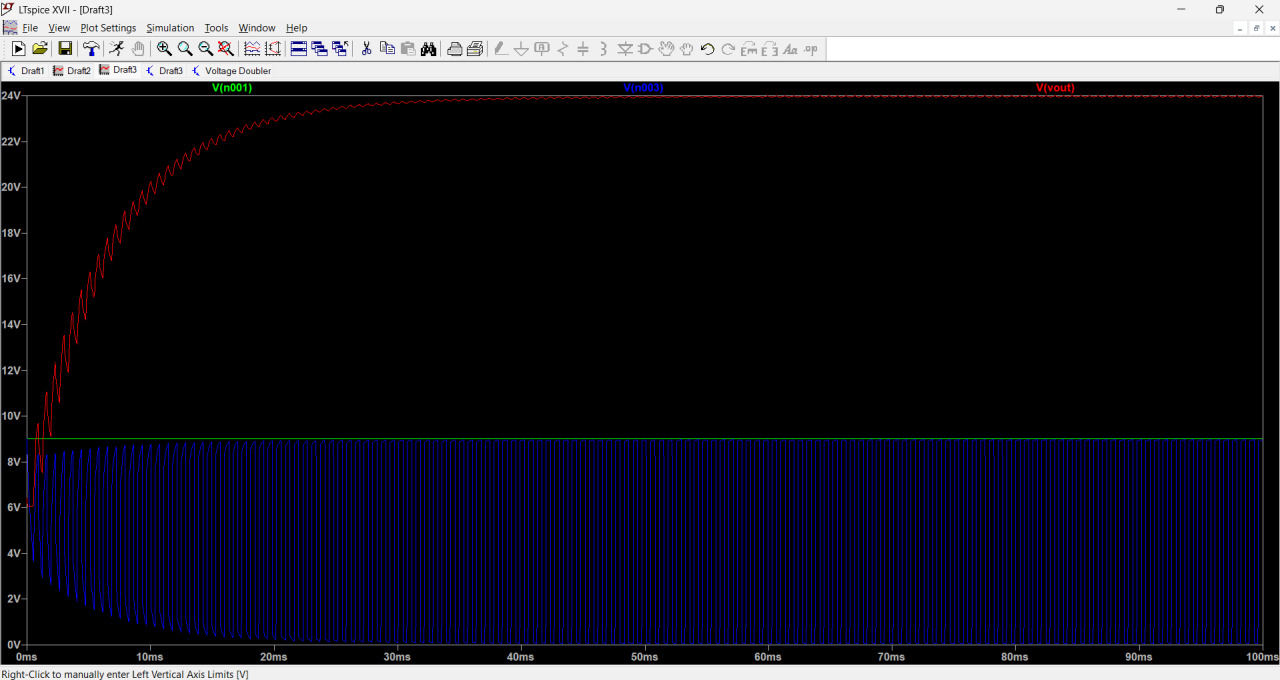
Final Output
- The output is not 27 V.
- It is approximately ~24 V (27- 4 * 0.7 V = ~ 24 V).
Task 4: The Power Shuffle: Buck-Boost Edition
- Objective: To learn about the DC-DC Converters
- Task: Learn about Boost and Buck converters and perform the following:
- Build a 1.5V to 5V DC-DC Boost converter
- Build a 12V to 5V DC-DC Buck converter
- Platform: LTSpice
- Task: Learn about Boost and Buck converters and perform the following:
Boost Converter
What is a Boost Converter?
A boost converter is a circuit that steps up or increases a lower input DC voltage to a higher output DC voltage.

Components:
-
Input Voltage Source (V1 = 1.5V): This is the DC supply that we want to boost to a higher voltage.
-
Inductor (L1 = 180 µH): Stores energy when the switch is closed
-
Switch (S1): A controlled switch using a model .model MYSW SW(...). It is controlled by the PWM square wave from voltage source Vsq.
-
PWM Source (Vsq): A pulse signal that turns the switch ON and OFF at high frequency.
- Defined as PULSE(0 5 2.5n 500p 500p 0.1m 0.2m): ON time = 0.1ms, OFF time = 0.1ms ⇒ 50% duty cycle, frequency ≈ 5 kHz
-
Diode (D1): Prevents current from flowing back into the inductor.
-
Output Capacitor (C1 = 33 µF): Smooths the boosted output voltage.
-
Load Resistor (R1 = 150 Ω): Represents the load drawing power from the boosted output.
Working Principle:
-
Switch ON (S1 closed):
- Inductor L1 is directly connected to Vin.
- Inductor stores energy in its magnetic field.
- Diode D1 blocks current from flowing to the output.
-
Switch OFF (S1 open):
- The inductor’s magnetic field collapses, and its polarity reverses.
- This causes a voltage greater than Vin to appear across the inductor.
- This high voltage pushes current through D1, charging C1 and powering the load.
-
Voltage Boost:
- The average output voltage increases depending on the duty cycle (D) of the switch.
- The circuit works on the basis of Discontinuous mode of Conduction because the current in the inductor drop to some extent when the switch of open.
- Therefore the Ideal output voltage not only depends on the duty cycle but other parameters also.

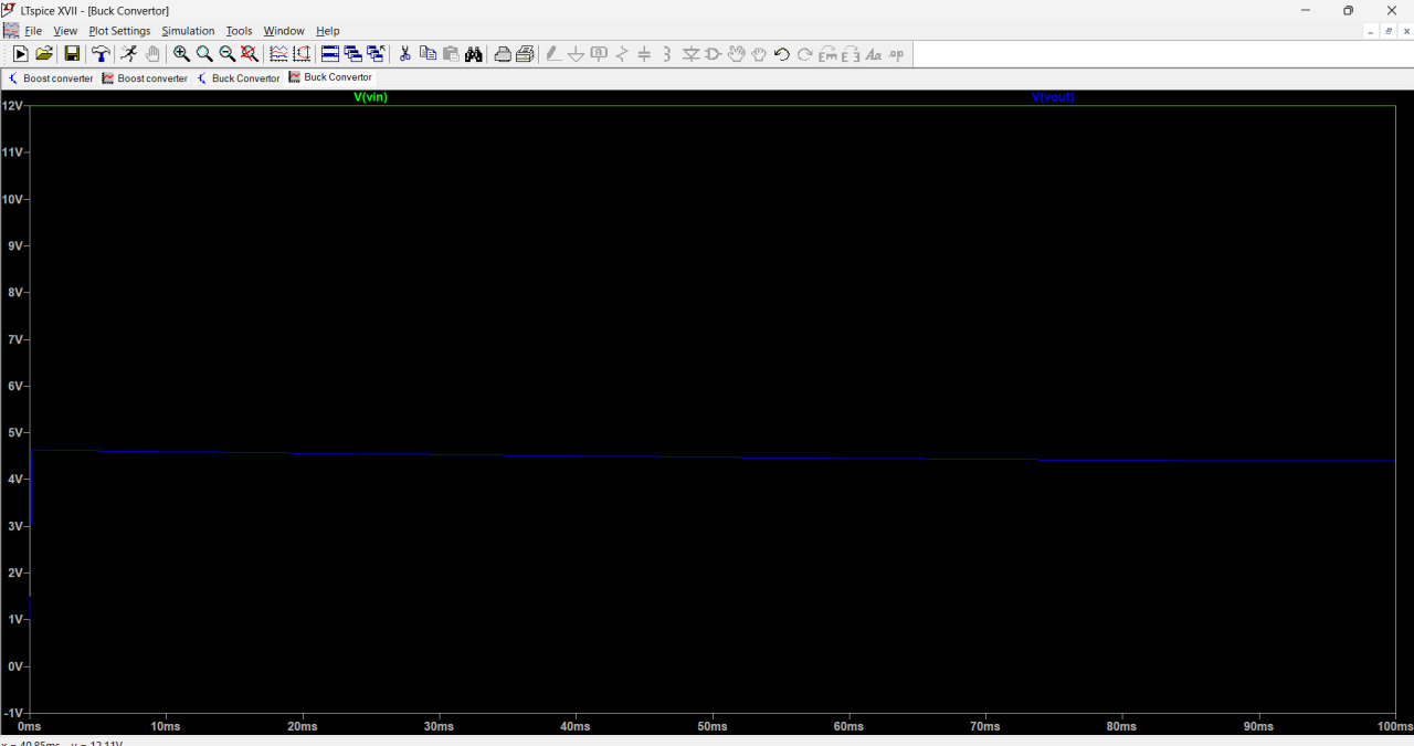
Buck Convertor
What is a Buck Convertor?
A buck converter is a circuit that steps down or decreases a higher input DC voltage to a lower output DC voltage.
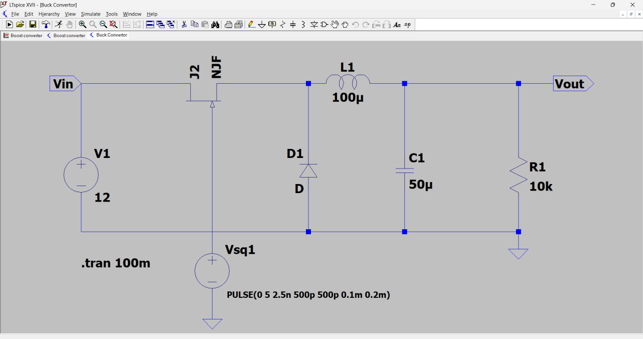
Components:
- V1 = 12 V (Input voltage)
- L1 = 100 μH (Inductor)
- D1 (Diode)
- C1 = 50 μF (Output capacitor)
- R1 = 10 kΩ (Load resistor)
- Vsq1 (PULSE) Switching signal to drive the buck converter
- J2-NJF (switch) Controlled by Vsq1
Working:
When the switch is ON:
- Current flows through the inductor and switch.
- The inductor stores energy by building a magnetic field.
- The inductor’s polarity opposes the input voltage.
- As a result, less voltage reaches the output.
When the switch is OFF:
- The inductor’s magnetic field collapses.
- It releases stored energy and current flows from the inductor through the diode to the capacitor and load.
- This increases the output voltage and maintains the current at the output, so that the circuit does not collapse.
Click here for the part 2 of the report