BLOG · 11/5/2025
Part 2 of MARVEL Level 1

Task 5: 4 Bits to Rule Them All
Objective:
- To design and implement a 4-bit Arithmetic Logic Unit (ALU) in CircuitVerse such that the ALU should perform the following operations: addition, subtraction (using 2’s complement), and logical operations (AND, OR, XOR).
- To design a control unit to select the desired operation based on input signals and display the result along with any carry/overflow flags when applicable.
1 Bit Full Adder
A 1-bit full adder is a digital circuit that adds two binary digits and also takes in a carry from a previous addition. It gives two outputs: a sum and a carry out.

Truth Table:
| A | B | Cin | Sum | Cout |
|---|---|---|---|---|
| 0 | 0 | 0 | 0 | 0 |
| 0 | 0 | 1 | 1 | 0 |
| 0 | 1 | 0 | 1 | 0 |
| 0 | 1 | 1 | 0 | 1 |
| 1 | 0 | 0 | 1 | 0 |
| 1 | 0 | 1 | 0 | 1 |
| 1 | 1 | 0 | 0 | 1 |
| 1 | 1 | 1 | 1 | 1 |
Click here to redirect to the 1 bit Full Adder
4 bit full Adder:
A 4-bit full adder can be built by connecting four 1-bit full adders in series, where the carry-out of each adder becomes the carry-in of the next.
The subtraction (2's complement) operation is implemented in the same full adder circuit by by XORing the B with Subtraction bit (1).
4 Bit ALU

Components Used:
- 4 bit Full Adder: Used in arithmetic operations like addition and subtraction.
- Multiplexer (MUX): Select between different operations (e.g., AND vs ADD).
- Selects the operation to perform AND, OR, ADD, SUB, etc.
- Based on the control inputs, it routes the correct operation's output to the final ALU output.
- MUX implements operation control, but only for data selection.
- Logic gates: Perform bitwise operations like AND, OR, NOT.
How It Works:
- Inputs: Two 4-bit numbers (
A[3:0],B[3:0]) and control signals. - 1-bit ALU: Each bit of A and B is processed by a 1-bit ALU (4 in total, chained together).
- Operation Selection: Logic operations like AND, OR, NOT use logic gates and Arithmetic operations like ADD, SUB use full adders.
- Carry Handling: The carry-out from one bit is passed as carry-in to the next FA block.
- Zero Flag: Returns the status output from the ALU that tells whether the result of the operation is zero.
- Output: Final result is a 4-bit output.
Click here to redirect to the 4 bit ALU
Task 6: Whose Array Is It Anyway?
- Objective: To understand and implement combinational logic design using PAL and PLA structures.
- Tasks:
- Read up on basics of PROM, Programmable Logic Arrays and Programmable Array Logics and understand the key differences.
- Design a logic circuit that outputs '1' if the number of 1’s in a 3-bit input (A, B, C) is odd.
- First designing using a PAL.
- Then same thing using a PLA.
- Draw fuse tables of AND Array and OR Array and show the fuse and blown connections.
- Design a controller that manages three lights in a smart home system based on these conditions - Motion sensor (M), Light level sensor (L), Time of day (T), Manual override (O) - using either PLA or PAL and justify the design.
- Platform: Logisim Evolution
PLD (Programmable Logic Device)
A Programmable Logic Device is an electronic component used to build digital circuits where the logic functions like AND, OR, NOT can be programmed by the user after manufacturing. PLDs are used to customize the digital logic in one chip.
Types:
- Simple PLDs - PROM, PLA, PAL
- Complex PLDs - Multiple PLAs or PLDs in a single chip
- FPGAs - Field Programmable Gate Arrays
What is an Array in a PLD?
An array refers to a grid-like structure where input lines and their complements intersect with logic gates through programmable connections like fuses.
Types:
AND Array
- Generates product terms (Minterms) - AND combinations of input variables.
OR Array
- Combines product terms to form the final sum-of-products output (OR of ANDs).
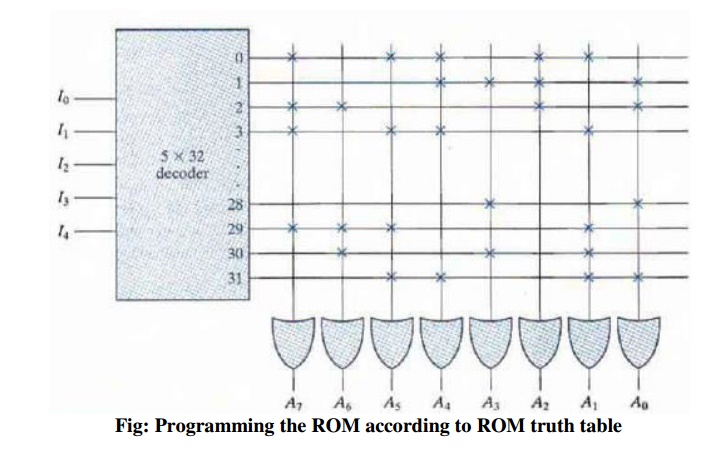
A) PROM (Programmable Read-Only Memory)
- It is a Fixed AND array and a programmable OR array.
- Commonly a Decoder.
- Originally meant for data storage, but also used to implement logic functions.
- AND array: Hard-wired (not changeable).
- OR array: Programmable fuses.
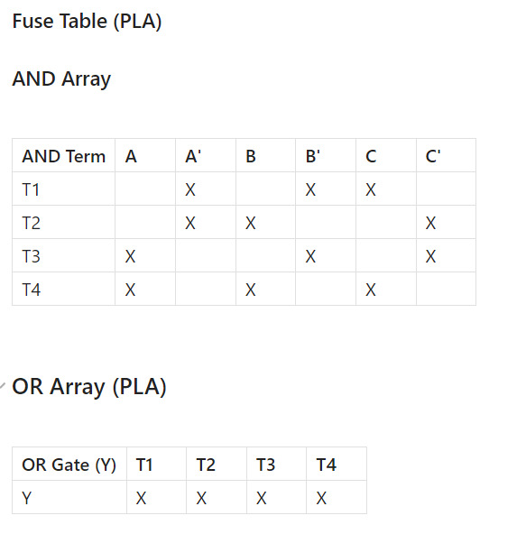
B) PLA (Programmable Logic Array)
- A fully programmable logic device.
- Both AND and OR arrays are programmable, giving maximum flexibility.
- AND array: Programmable
- OR array: Programmable.
- Suitable when you need to implement many complex logic expressions.
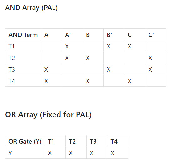
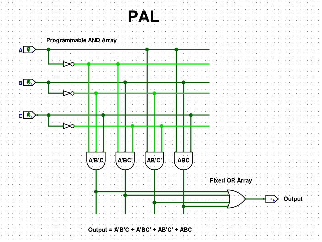
C) PAL (Programmable Array Logic)
- It is a simplified version of PLA.
- Programmable AND array, but a fixed OR array.
- Faster and less expensive than PLA, but less flexible.
- AND array: Programmable
- OR array: Fixed
- Useful when speed is more important than flexibility.
- Works well for simpler logic functions with fewer product terms.
D) Designing a logic circuit that outputs '1' if the number of 1’s in a 3-bit input (A, B, C) is odd
Truth Table:
| A | B | C | Output (Y) |
|---|---|---|---|
| 0 | 0 | 0 | 0 |
| 0 | 0 | 1 | 1 |
| 0 | 1 | 0 | 1 |
| 0 | 1 | 1 | 0 |
| 1 | 0 | 0 | 1 |
| 1 | 0 | 1 | 0 |
| 1 | 1 | 0 | 0 |
| 1 | 1 | 1 | 1 |
So the output is 1 for:
- 001
- 010
- 100
- 111
Simplify Boolean Expression (Sum of Minterms)
From the truth table:
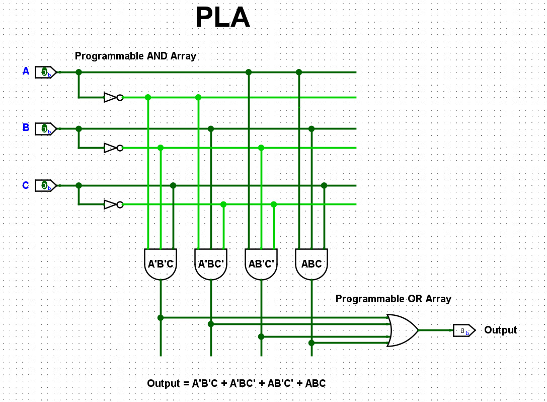
Y = A'B'C + A'BC' + AB'C' + ABC
This is a minimized SOP form.
Design Using PAL:
- AND array is programmable
- OR array is fixed
AND Array Minterms
- A'B'C
- A'BC'
- AB'C'
- ABC
Fuse Table (PAL)
Each row is an AND gate. An X means a connection (fuse intact). Blank means blown.
PAL Diagram
Design Using PLA (Programmable Logic Array)
In PLA,
- Both AND and OR arrays are programmable
We use the same 4 minterms.
Fuse Table (PLA)
PLA Diagram
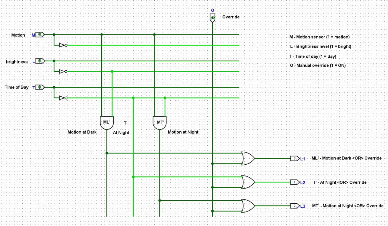
E) Design a controller that manages three lights in a smart home system based on these conditions - Motion sensor (M), Light level sensor (L), Time of day (T), Manual override (O) - using either PLA or PAL and justify the design.
Inputs:
| Symbol | Meaning |
|---|---|
| M | Motion sensor (1 = motion) |
| L | Light level (1 = bright) |
| T | Time of day (1 = day) |
| O | Manual override (1 = ON) |
Outputs:
| Light | Controlled by |
|---|---|
| L1 | Motion in dark OR manual override => L1 = M·L' + O |
| L2 | Night OR manual override => L2 = T' + O |
| L3 | Motion at night OR manual override => L3 = M·T' + O |
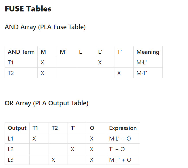
Product Terms (Minterms):
| AND Term | Expression | Meaning |
|---|---|---|
| T1 | M·L' | Motion and darkness |
| T2 | T' | Night time |
| T3 | O | Manual override |
| T4 | M·T' | Motion at night |
FUSE Tables
PLA Diagram
Task 7: Your Logic, Preloaded
Objective: To understand the concept of Look-Up Tables (LUTs)
- Tasks:
- Read up on basics of Look Up Tables in digital electronics
- Implement a 2-input XOR function using a 4x1 LUT (2 input bits select one of 4 pre-stored outputs).
- First, manually create the truth table for XOR.
- Then, program a 4x1 LUT with the correct outputs based on the truth table.
- Simulate how inputs select different stored outputs.
- Platform: Logisim Evolution
What is a Look up Table?
- A Look-Up Table (LUT) is a simple memory-based device that stores outputs for every possible combination of inputs to a logic function.
- Inputs are treated as a binary address.
- Each address points to a memory location where the correct output is stored.
- The output is fetched from memory instead of being calculated live.
LUTs are used in:
- In ROMs
- . In FPGAs (Field Programmable Gate Arrays):
- FPGAs are made up of thousands of LUTs.
- A typical LUT4 (4-input LUT) can implement any logic function of 4 inputs.
- Programmers configure the LUT contents to define the desired logic.
ROM Setup
Treat A and B as a 2-bit address (A is MSB, B is LSB).
| Address (A B) | Decimal Address | XOR Result | Stored in ROM |
|---|---|---|---|
| 00 | 0 | 0 | ROM[0] = 0 |
| 01 | 1 | 1 | ROM[1] = 1 |
| 10 | 2 | 1 | ROM[2] = 1 |
| 11 | 3 | 0 | ROM[3] = 0 |
- You connect inputs A and B to the address lines of the ROM.
- Based on the values of A and B, the ROM goes to that memory address.
- The ROM outputs the stored value (the XOR result) at that address.
4x1 LUT in Logisim Evolution

Task 8: Engineer’s Swiss Army Knife
Objective: Create a Matlab account and complete the MATLAB Onramp course and obtain the certification.
1. Basic Syntax
- Assign values: x = pi
- Call functions with input: y = sin(-5)
2. Desktop Management
- save/load: Save/load workspace to/from .mat file (save filename, load filename)
- clear/clc: Clear variables or command window
3. Array Types
- Scalar: 4
- Row vector: [3 5]
- Column vector: [1; 3]
- Matrix: [3 4 5; 6 7 8]
4. Evenly Spaced Vectors
- Colon operator: 1:4, 1:0.5:4
- linspace(1,10,5): Create 5 equally spaced values between 1 and 10
5. Matrix Creation
- rand(2): 2×2 matrix with random values
- zeros(2,3): 2×3 matrix of 0s
- ones(2,3): 2×3 matrix of 1s
6. Array Indexing
-
Array: A collection of numbers arranged in rows and columns.
-
Index: Position of an element in an array.
-
Indexing: Accessing elements of an array using position numbers.
-
A(end,2): Last row, second column
-
A(2,:): Entire second row
-
A(1:3,:): First 3 rows
-
A(2) = 11: Modify value
7. Array Operations
- Addition: [1 2; 3 4] + 1
- Matrix multiplication: [1 1; 1 1] * [2 2; 2 2]
- Element-wise: [1 1; 1 1] .* [2 2; 2 2]
8. Multiple Outputs
- [xrow, xcol] = size(x): Rows and columns
- [xMax, idx] = max(x): Max value and its index
9. Documentation
- doc randi: Open documentation for a function
10. Plots
- plot(x,y,"ro--",LineWidth=5): Plot line with red dashed style and circle markers
- hold on/off: Add to or reset plots. Can plot one line on top of another in the same axes by using the hold on command.
- title, xlabel, ylabel, legend: Add titles, labels, legends
11. Tables
- data.HeightYards: Access a table variable
- data.HeightMeters = data.HeightYards * 0.9144: Create derived variable
12. Logical Indexing
- [5 10 15] > 12: Compare values
- v1(v1 > 6): Filter elements
- x(x == 999) = 1: Replace values conditionally
13. Programming
- If-Else:
- For Loop: for c = 1:3 >> disp(c) >> end