
RESOURCE · 4/6/2025
FPGA for Starters
A complete beginner’s guide to writing, testing, and deploying your first digital design.

Introduction
Ever wondered how digital circuits come to life on real hardware?
In this resource article , you'll design a full adder using Verilog, simulate it, and program it onto an FPGA board.
We’ll use the Basys 3 and Arty A7 35T FPGA development boards and explore how this tiny board lets you shape hardware with code.
Prerequisites
Before jumping into FPGA design, make sure you're equipped with the right knowledge and tools.
- Basic understanding of digital logic and combinational circuits .
- Basys 3/Arty A7 FPGA Development Board ( available in MARVEL) .
- A micro-USB cable for board connection.
- Xilinx Vivado Design Suite-This is the platform we will use to design,simulate and program FPGAs.
- Digilent Adept - It contains necessary Hardware Drivers
Also recommended : Good understanding of Hardware Description Language like Verilog.
Intro to FPGAs
An FPGA, or Field Programmable Gate Array, is a special type of chip that you can customize to act like any digital circuit you want using code. While regular computers and microcontrollers run instructions one after another like following a recipe, an FPGA can perform many tasks all at once, because it doesn’t run software , it becomes the hardware you describe. You write that behavior using special languages like Verilog or VHDL , and software like Vivado or Modelsim turns your code into a file that configures the chip’s internal wiring. FPGAs are used in areas where speed, precision, and customization really matter , like in medical equipment, satellites, self-driving cars, or even video game consoles.
Basically , it is an empty slate that you can design ANY digital circuit on , from a basic AND gate to an entire CPU , FPGAs are highly flexible devices .
Basys 3
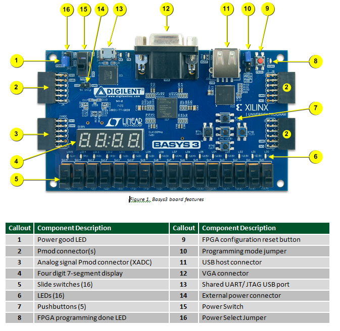
The Basys 3 is an entry-level FPGA development board designed by Digilent, powered by the Xilinx Artix-7 (35T) FPGA. It’s ideal for students, hobbyists, and anyone beginning their journey into digital design and hardware description languages like Verilog. The board features built-in peripherals such as 16 slide switches, 16 LEDs, 5 push buttons, 4 seven-segment displays, and a VGA port—allowing users to create and test logic circuits without connecting any external hardware. Its USB-JTAG interface enables easy programming through Vivado, making it a self-contained and user-friendly platform for learning and prototyping.
Arty A7 35T
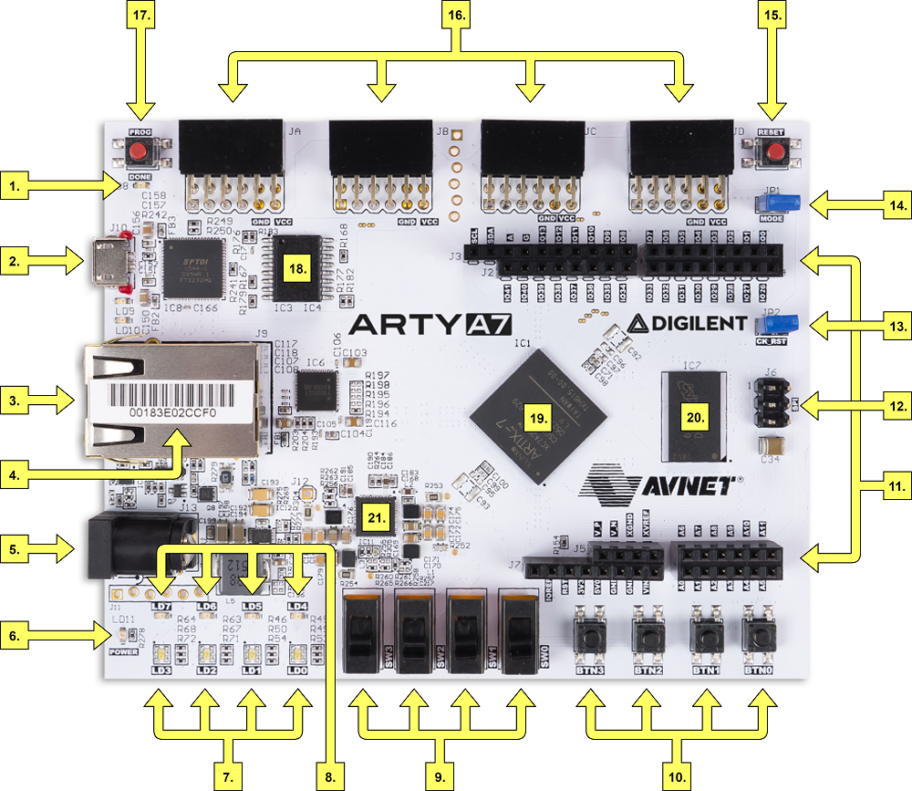 The Arty A7-35T, also by Digilent, is a more powerful and flexible FPGA board aimed at intermediate to advanced users. It’s built around the same Xilinx Artix-7 (35T) FPGA but focuses on expandability and embedded system development. The board includes multiple Pmod ports, 512MB of DDR3 RAM, a MicroSD card slot, and USB interfaces for JTAG and UART communication. Unlike the Basys 3, it has few onboard I/O like switches or LEDs, encouraging users to build modular systems by interfacing with external peripherals.
Setting up the Environment
Assumption: You have already Installed Digilent Adept and Vivado.
Step 1: First Let us download the board Files Download
Step 2:
Now when you open the .zip file and navigate to
vivado-boards-master\new\board_files
, you should see this :

Select the folder named as basys3 and artu-a7-35 , copy and paste them in
Vivado\2024.2\data\boards\board_files
Create board_files manually if not present.
It should look like this:

Step 3: Open Vivado Design Suite , don't worry , it usually takes half a minute to load.

This will be what you see when you open Vivado , click Create Project , type project Name , keep clicking next , do not add any files or sources , for project type choose RTL project and continue.
Step 4: Choose part
Now you will be asked to choose part/board . Click Boards in top left and you should see this:

For this project , Choose Basys3 and click next . Step 5: Now you should see this window:

Click Finish . Now your project is set up and we can start working on it.
Designing The Circuit
Let's implement a Full Adder . First , we describe the logic of the full adder or any circuit we need in a language called Verilog . It can be used to build large and complex digital circuits for signal processing , computing , communication etc . There is virtually nothing that you cannot program an FPGA to do in the domain of digital electronics. This is achieved by HDL ( Hardware Description Language ) . Verilog and VHDL are some of the most common ones.
As you all must know , a full adder is nothing but a combinational circuit that takes 3 inputs , adds them and gives 2 outputs , sum and carry .
If we apply the common full adder logic in Verilog , we can write the following code :
module full_adder(a,b,c,sum,carry);
input a,b,c;
output sum,carry;
assign sum = a^b^c;
assign carry = (a&b)|(b&c)|(a&c);
endmodule
The module(or program) is named full_adder with inputs a,b,c and outputs sum,carry .
Using the "assign" statement , values or functions can be assigned to output.
Here the symbol "^" represents XOR gate , "|" represents OR gate and "&" represents AND gate.
Now that we know how to write the verilog code , let's move on to simulating and verifying it .
In HDL programming , the program or module only describes the functionality of the circuit , or in other words , "what it should do". However , the module by itself does not execute the program or test it . We have to write a separate program called a testbench , where you "import" or technically , instantiaze the circuit module (in this case , full_adder) and give input signals and record the output signals and verify it manually . Testbenches are also written in verilog or whichever language the circuit module is written in.
Testbench:
module full_adder_testbench();
reg a,b,c;
wire sum,carry;
full_adder uut(.a(a),.b(b),.c(c),.sum(sum).carry(carry));
initial begin
a=0;b=0;c=0;#10
a=0;b=0;c=1;#10
a=0;b=1;c=0;#10
a=0;b=1;c=1;#10
a=1;b=0;c=0;#10
a=1;b=0;c=1;#10
a=1;b=1;c=0;#10
a=1;b=1;c=1;#10
end
endmodule
This code basically depicts the Truth Table for the inputs of the full_adder , and after every iteration of inputs , there is a `#10` time delay before the next inputs are given , so that there is enough time delay for the output to be recorded .
In Vivado , the circuit module ( Program that describes the circuit aka full_adder) is referred to as a Design Source , and the testbench is referred to as Simulation source.
Constraints
A constraint file in Vivado is like a map that tells the FPGA which physical pins on the chip should be connected to the inputs and outputs defined in your Verilog code. Your code might say "led" or "button", but the FPGA needs to know exactly which pin on the board that refers to , this is what the constraint file specifies. It ensures your design actually interacts with the real-world components like switches, LEDs, or sensors connected to the board. Without this file, the FPGA wouldn’t know how to link your logic to the physical hardware.
The constraint file (.xdc file in Vivado ) is board-specific , that is , each board has a specific constraint file .
The general practice is , to save a copy of the Master Constraint file , in which all ports are declared but it is commented , so that only the ports we require , we can uncomment it and declare it .
Here is the master constraint file for Basys3 and Arty A7 .
First , let us decide what ports we will use . For inputs a, b and c , I will use sliders(switch) sw[0], sw[1] and sw[2] respectively , and for outputs sum, carry I will use led[0] and led[1].
I will uncomment the lines that declares ports sw[0] , sw[1] , sw[2] , led[0] amd led[1] .
Now , I will replace the port name with the name of the port declared in the verilog module .
Example: replace sw[0] with a .
Note: The port name has to be exactly the name of the ports used in the verilog module.
After uncommenting and replacing with the correct name for all the ports, and then removing all commented lines (optional) , the constraint file should look like :
#Switches
set_property PACKAGE_PIN V17 [get_ports {a}]
set_property IOSTANDARD LVCMOS33 [get_ports {a}]
set_property PACKAGE_PIN V16 [get_ports {b}]
set_property IOSTANDARD LVCMOS33 [get_ports {b}]
set_property PACKAGE_PIN W16 [get_ports {c}]
set_property IOSTANDARD LVCMOS33 [get_ports {c}]
#LEDs
set_property PACKAGE_PIN U16 [get_ports {sum}]
set_property IOSTANDARD LVCMOS33 [get_ports {sum}]
set_property PACKAGE_PIN E19 [get_ports {carry}]
set_property IOSTANDARD LVCMOS33 [get_ports {carry}]
Now we are Ready to start programming the FPGA:
Programming the FPGA
After creating project , you would be taken to the project manager window:

The right side is the project summary , where you can check if you have chosen the correct board . The left side is the sources tab , here you will create the design source , simulation source and constraint source.
Click on the + icon in the sources tab ,

Now create a design source :

Name the source as full_adder and click finish , do not add any input or output.
Now the source file will open up with some comments and module name , remove all of it until the file is empty , and then paste the code of verilog module (full_adder) described earlier .
Similarly create simulation source and paste the testbench code ( full_adder_tb) and do the same for the constraint source as well.
Now we are ready to simulate and program the FPGA .
In the left corner of the project manager , we can see the flow navigator :

Click Run Simulation->Behavioral Simulation .
This will generate a wave form where you can manually verify the output:

After this , click Run Synthesis , once it is done , click Run Implementation .
Now , at the bottom of the flow navigator , click Generate Bitsream , a dialog box will open , just click next . Once it shows done , open Hardware Manager
 However , before continuing , ensure that the FPGA is configured this way:
- The Program mode Jumper is set to JTAG

- The Power mode jumper is set to USB
 Click
Click Open Targetand chooseautoselect, if the FPGA is connected to the right port ( It should be switched ON ) , you will get this:

If this doesn't show , try connecting to different USB ports in your system.
Now click program device :
 And choose the right bitstream ( in case of multiple files ) and click
 Program .
That's IT!!! Now you have succesfully programmed your first ever FPGA !
To check if the programming is done properly , check if the Programming done LED is on , that means the FPGA has been succesfully programmed .
You can toggle the sliders and check how the output LEDs vary to ensure it behaves like a Full Adder .
With your design complete, constraints applied, and the bitstream successfully loaded onto the FPGA, you’ve just taken a full digital circuit from code to physical hardware. The Full Adder you built is now blinking on your board—proving that your Verilog logic is alive and working! This hands-on process forms the foundation of countless complex projects you’ll be able to build in the future.When using any other board like Arty A7 , the only thing that changes is the constraint file .
Here is a video of my Implementation of Full Adder:
Conclusion
In this article, we took a complete walk through the FPGA design journey from understanding the FPGA (Basys 3 and Arty A7), writing Verilog code, simulating it, applying constraints, and finally programming it onto a real board. Along the way, you’ve learned not just how to build a Full Adder, but how to think in hardware, debug systematically, and use industry-standard tools like Vivado. While this was a simple project, it opens the door to building more complex designs like counters, ALUs, state machines, and even processors. With your first successful implementation behind you, you're now equipped to take on bigger and more exciting challenges in digital design. Keep experimenting, and happy building!
Thank You!
Additional Resources for Exploration