RESOURCE · 16/3/2023
Challenges in Sub 1nm Process
As the nodes are shrinking, we take a look at the new challenges that arise.
 | OP |
RESOURCE · 16/3/2023
As the nodes are shrinking, we take a look at the new challenges that arise.
| OP |
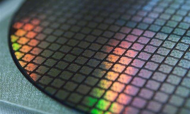
 \n\nFig. Silicon Wafer (Credits: Google)\n\n\nThe sub 1nm process refers to the next generation of semiconductor manufacturing technology, which involves creating transistors and other components that are smaller than 1 nanometer in size. The sub 1nm process is still in the research and development stage, and there are several challenges that need to be overcome before it can be commercialised. Some of the key challenges include:\n\n## Atomic-level precision\n\nThe sub 1nm process requires extreme precision at the atomic level to create the desired structures. This precision must be maintained throughout the entire manufacturing process, from deposition to patterning and etching.\n\n
 \n\nFig. Images of Silicon Wafer under scanning electron microscope (Credits: Wiley)\n\n## Materials and process compatibility\n\nThe materials and processes used in the sub 1nm process must be compatible with each other and with the existing infrastructure. This is a significant challenge, as many of the materials and processes used in current semiconductor manufacturing are not suitable for sub 1nm processes.\n\n
 \n\nFig. Cross-sectional SEM image of the Si wafer following lithiation at a fixed current density Credits: Michael Cohn-Research Gate)\n\n## Manufacturing cost\n\nThe sub 1nm process is likely to be much more expensive than current semiconductor manufacturing processes, due to the increased complexity and precision required. This could limit the commercial viability of sub 1nm technology.\n\n
 \n\nFig. Increasing Cost for every smaller Process Node (Credits:SemiEngineering)\n\n## Device variability \n\nAs devices become smaller and more complex, they become more susceptible to variability, which can affect their performance and reliability. The sub 1nm process must address this challenge by developing techniques to minimise variability and improve yield.\n\n
 \n\nFig. Size Variability of each die (Credits: Yufei Xing Research Gate)\n\n## Heat dissipation \n\nAs devices become smaller, the amount of heat generated per unit area increases. This can lead to thermal issues that can affect device performance and reliability. The sub 1nm process must develop new techniques for heat dissipation to ensure reliable operation.\n\n
 \n\nFig. Heat Simulation of Wafers (Credits: CreateLimit Co.)\nOverall, the sub 1nm process presents significant technical and economic challenges, but also promises significant benefits in terms of increased computing power, reduced power consumption, and new applications.\n\n### References\n[^1]: About Semiconductor Chips\n\n[^2]: The Sillicon Wafer