
BLOG · 13/6/2025
PCB Revolution

This Article is yet to be approved by a Coordinator.
Task 8: The PCB Revolution
What is PCB Design?
- PCB, Printed Circuit Board, connects electronic components together. It is used in all electronics like phones, laptops, cars, satellites, etc.
Why PCB Design Matters
- Ensures reliable, low-noise connections between chips. It allows large-scale production of electronic products. It helps organize complex circuits into a compact, layered board.
Some of the PCB Designing Software and Simulation Tools
- Altium Designer, KiCad, Eagle (by Autodesk), OrCAD (by Cadence)
- LTspice, PSpice, Multisim, Simulink (with Simscape Electrical), ANSYS Electronics Desktop
Basic PCB Terms
- Components: These are the electronic parts like resistors, capacitors, and chips that are placed on the board.
- Printed Circuit Board (PCB): The empty board made of layers and copper – no components attached yet.
- PCB Layout: A digital design that shows where each part and wire (trace) goes on the board.
- Trace: The thin copper line on a PCB that connects different components together (like wires on the board).
- Pads are small metal areas on the PCB where component pins are soldered. They serve as the contact points between the component and the copper traces.
- Layers: PCBs have multiple levels (layers) inside them.
- Signal layers: carry traces (connections).
- Plane layers: are large copper areas, usually for power or ground. - It provides shielding against external noise originating from radio frequency sources and it provides a path for heat transport away from hot components.
- Multilayer PCB: A PCB with more than two copper layers – used for complex circuits.
- PCB Stackup: The way all the layers (copper and insulating material) are arranged in the board. PCB thickness is about 1.57 mm.
- Schematic Sheets: Drawings that show how each component is connected — like a blueprint before building.
- PCB Fabrication: The process of making the actual board by adding copper layers and cutting it to shape — no parts yet.
- PCB Assembly (PCBA): Putting the components on the board by soldering them.
- PCBA = the finished board with all parts on it.
- PCB assembly = the process of assembling it.
- Solder mask = The top layer of a PCB is called the “solder mask”. This layer is used to define the locations where solder will be applied for PCB assembly.
- Silkscreen = If you look at the surface of a PCBA, you’ll usually see some letters, numbers, or logos printed on the board. This material is called “silk screen”.
- PCB Laminate: The strong, non-conductive material (like fiberglass) between copper layers that holds the board together.
Main Files You Create in a PCB Design
1. Schematic Sheets:
- Schematic sheets are like circuit diagrams, they show how components are connected electrically.
- They show what connects to what, but not how things are placed on the board.
- It shows/contains: All the components used (resistors, chips, etc.), electrical connections (called nets), power and ground lines and connections across different schematic pages (using ports or net names)
- It does not show/contain: Physical positions of parts, actual paths like traces, vias, or planes, details on how power flows through copper and routing details
There are two main ways to organize schematics in PCB design:
- Flat schematics: All parts are shown on one big set of sheets without special grouping.
- Hierarchical schematics: Schematics are organized in levels or blocks, showing how smaller parts connect inside bigger sections.
2. Bill of Materials (BOM)
- A list of all components used in your PCB design.
- It is created automatically by your ECAD software as you add parts.
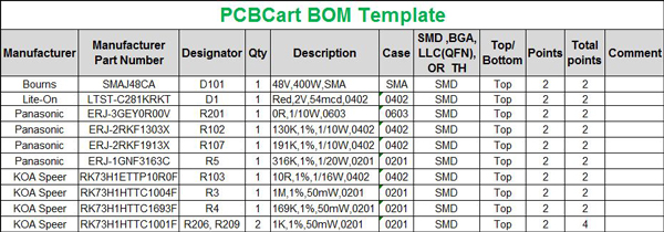
What’s in the BOM?
- Each component type gets a row.
- It shows:
- Part name
- Reference designators (like U33, R1, C5)
- Quantity
- Part number
- Description
- Exported as PDF or Excel.
3. PCB Layout
What is PCB Layout?
It’s the physical design of your circuit board — shows where each part goes and how they’re connected with copper. It also includes the PCB stackup.
What’s in a PCB Layout File?
- Component footprints (pads, shapes, labels)
- Stackup info (number of layers, thickness, material types)
- Copper traces that connect components
- It includes a 3D view of the final board
4. PCB Libraries
What’s Inside a Library?
- Symbols (for schematics)
- Footprints (for PCB layout)
- 3D models
- Part info (like part numbers, descriptions)
Anatomy of Schematic
- Net: A net is the name for an electrical connection between two or more parts in a circuit. If you don’t name a net, the software will name it for you.
- Power and Ground Ports: Power and ground ports define how voltage and ground are connected across your circuit.
- Notes: Notes in schematics are used to give extra information, such as Design changes in the project.
- Multi-port symbol: Some big components, like processors, have too many pins to fit in one symbol in a schematic. So, they are split into multiple parts, called a multi-part symbol.
- Input: Receives data. Output: Sends data. Bi-directional: Can do both
- Ports: When a design has many schematic sheets, you use ports to connect signals between sheets.
In Altium Designer, you can use the Manufacturer Part Search panel to find components for your design. You can search by type, part number, manufacturer, or keywords. If you don’t want to search for parts inside Altium, you can use websites like Octopart.
How to place components in schematic
When placing components in a schematic:
- Arrange inputs on the left, outputs on the right.
- Group parts that work together close to each other.
- Avoid crossing wires to keep the schematic clear.
- Use net names and ports instead of lots of wires crossing.
- Use special power and ground symbols for power connections.
- Split big circuits into multiple sheets if needed, linking them with ports.
- For big chips with many pins, use net names and ports to keep wiring simple.
Different types of reviewing the design
- Design rule check (DRC)
- Functional review
- Supply chain review
- Mechanical review
- Application review
PCB Design flow
- Schematic design and mechanical design are performed before PCB layout, oftentimes in parallel
- Any constraints on component placement, component sizes, board size, and mounting hole location are determined
- The designer implements the required board shape and mounting style in the new layout
- Components are arranged and checked against the size/height limits imposed by the enclosure
- After replacing or moving any components, the design is routed and the layout and evaluated
Which Components to Place First?
- Large processors: These components will make a lot of connections to other components, so they should be centrally located in the PCB layout.
- Power inputs: Every board needs power to operate.
- Connectors: Data connectors should be placed somewhere on the board, normally along the edge.
- Radio frequency (RF) components: The RF components in your design should have their own area where they can be confined so that they are kept away from digital signals.
Routing
Routing with Traces:
- Choose the Right Trace Width
- Keep Enough Space Between Traces - use 3W Rule: Space between two traces should be 3 times the trace width to reduce signal interference.
- Types of Traces: Microstrip, On the outer layers, above a ground plane. Stripline, On inner layers, between ground planes.
- Routing Angles: Use 45° angles for smooth, short routing.
- Use polygons (wider copper areas), not regular traces.
Routing with Polygons:
- Routing with polygons means using large copper areas (not thin lines) to connect parts of a circuit, especially for power (3.3V, 5V, 12V) and ground (GND) connections.
- Traces are narrow lines — good for small signals.
- Polygons are wide shapes — better for high current (like power lines).
- Polygons let you cover more area, connect many parts easily, and carry more current without overheating.
Routing with Vias:
Vias are small holes in a PCB that connect traces on different layers. Each via has:
- A drilled hole (where copper is plated inside)
- A pad (also called an annular ring) — the copper ring around the hole
- Minimum hole size: At least 8 mil diameter so any manufacturer can drill it.
Routing types of Signals:
- Single-ended traces: They are simple, it refers to a trace routed above a ground plane. The voltage carried by the signal in this case is measured between the trace and a ground plane.
- Differential pair: It uses two traces routed side-by-side to carry a digital or analog signal between two components. The signal is carried as two equal and opposite signals routed on the traces (V+ and V- in the above image), and the voltage carried by the signal is measured between the two traces.
I2C Routing (2 wires: SDA & SCL)
- Uses 2 lines: SCL = Clock. SDA = Data (2-way)
- One master, multiple peripherals devices
- Needs pull-up resistors (1kΩ or higher) on both lines to the power rail
- Keep traces short and narrow (≤10 cm, ~10 mil width)
- TVS (Transient Voltage Suppression) diodes can be added to protect I2C lines from static electricity (ESD) or sudden voltage spikes.
- One master, multiple slaves

SPI Routing
- Uses 3 or 4 lines: SCK = Clock, SDI = Data into controller, SDO = Data out from controller, CS = Chip Select (1 per device)
- Faster than I2C, no pull-up resistors needed
- Easy to route
- Can use series resistors (~22Ω) if traces are very long
- Each device gets its own CS line from controller
- Can contain multiple masters, but one master is active at a time.

UART Routing
- Uses 2 lines: TX = Transmitter, RX = Receiver
- One-to-one connection (no multiple devices)
- No clock line; works asynchronously
- Simple routing – just connect TX ↔ RX
- No impedance matching or resistors needed
- Can work well even over longer distances

**EMI (Electro Magnetic Interference)
What is EMI?
- It is the unwanted noise from electrical signals that can disturb other electronics. It happens due to bad PCB layout, poor grounding, or fast digital signals. It can be prevented by the use of filter circuits.
- Two types:
- Radiated EMI: Noise sent into the air like a radio waves. Caused by fast-changing signals creating electromagnetic waves.
- Conducted EMI: Noise traveling through wires/traces between devices. Can enter other circuits or systems.
Why EMI Matters?
Devices must pass EMC (Electromagnetic Compatibility) tests to be sold legally. Tests are done to ensure the device doesn't interfere with others or fail from external noise.
Electrostatic Discharge (ESD)
- A sudden shock (like a mini lightning bolt) when touching a metal part.
- Can damage components if not grounded properly.
- Common at connectors or exposed metal parts.
- Prevent it by, adding TVS diodes or ESD protection circuits.
**PCB Manufacturing
Once the PCB design is done, there are a few final steps before it can be fabricated and assembled.
- Final Design Cleanup: Review the design for any errors and remove unused items.
- Files Needed for Manufacturing:
- Gerber, ODB++, IPC-2581 files: Tell the factory how to make each layer.
- NC Drill File: Shows where to drill holes.
- Fabrication Drawing: Shows board dimensions, hole sizes, and stack-up info.
- Assembly Files (for placing parts):
- Bill of Materials (BOM): A list of all components (with quantity, part numbers, etc.).
- Pick-and-Place File: Tells machines where each component goes on the board.
- Assembly Drawing: A labeled drawing showing part locations and notes for assembly.
Fiducials
- Tiny copper marks at corners to help machines align the board during assembly.
DFM (Design for Manufacturing) Evaluation
- After you send your PCB files, the fabricator checks if the board can be manufactured reliably.
- They look for issues like: Too small pads or traces, Too-tight spacing between copper areas, Annular rings being too small, Incorrect hole sizes etc.
Panelization
- PCBs are not made one by one—they are made in large panels containing multiple boards. A panel is later cut (depanelized) into individual boards.
- Panels have standard sizes like: 18”×24”, 18”×12”, 9”×24”, etc.
- Depanelization (Cutting Boards Out of Panel): Cutting boards out of panel. Common methods are milling, v-scoring etc
**PCB Fabrication
It includes layer creation, drilling, copper plating, and applying solder mask and silkscreen.
Fabrication Steps
- Inner Layer Processing (For multilayer boards)
- Stencil Creation, Photoresist Coating, UV Exposure, Etching, Photoresist Removal, Roughening, Inspection
- Lamination
- All layers are stacked and pressed together at high temperature and pressure to form a solid board.
- Outer Layer Processing
- Drilling, Copper Deposition, Photoresist Coating & UV Exposure, Electroplating , Etching
- Final Steps
- Solder Mask, Surface Finish, Silkscreen Printing
